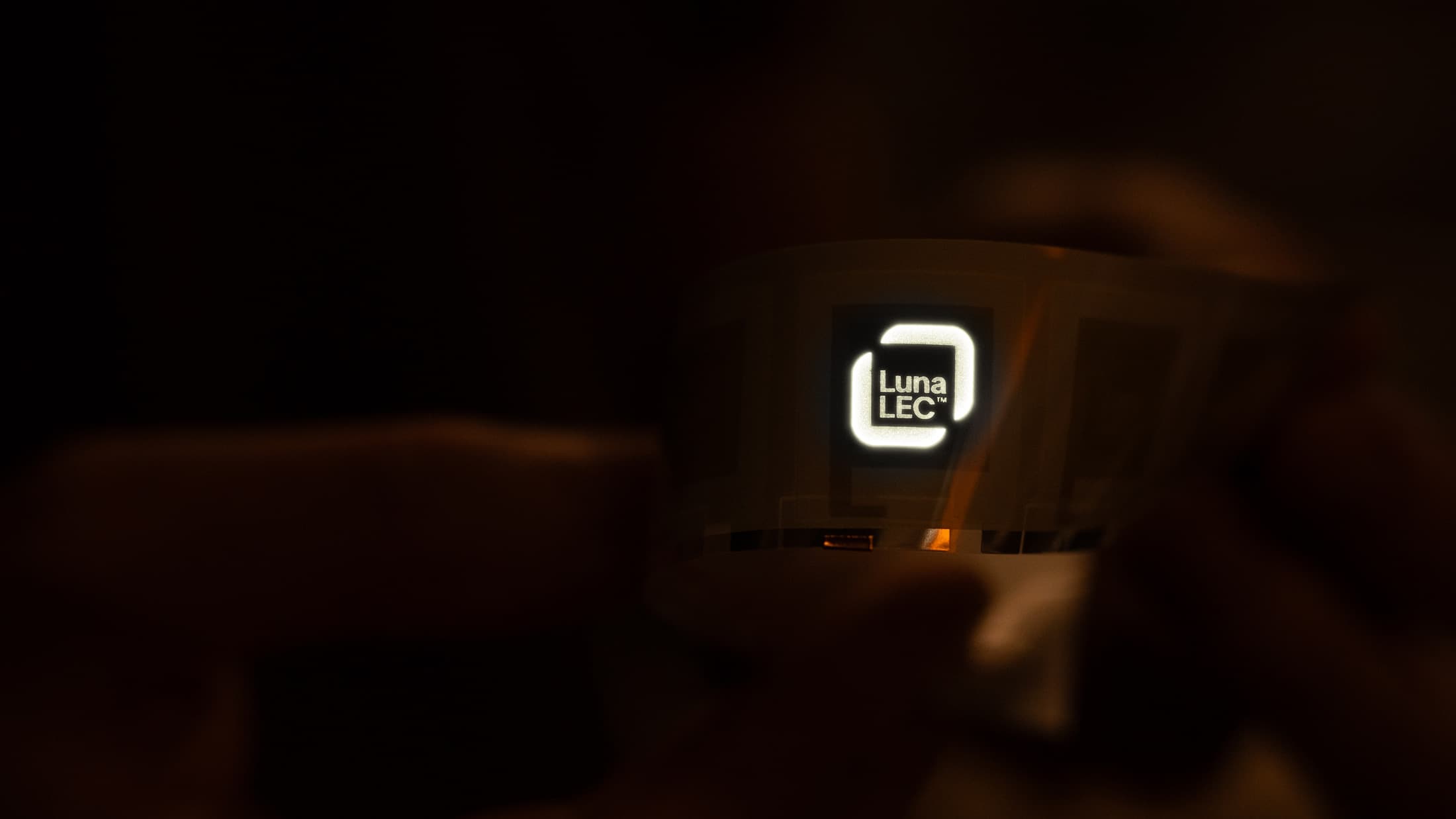
Understanding LEC
Light-emitting
Electrochemical Cells
The next revolution in lighting technology.
How It Works
The Science
What makes LEC technology fundamentally different from traditional lighting?
Current generation of LED and OLED generate light through a p-n junction built up by precise layers of semiconductors controlled to nanometer accuracy and achieving this level of molecular control requires energy and cost-intensive manufacturing processes.
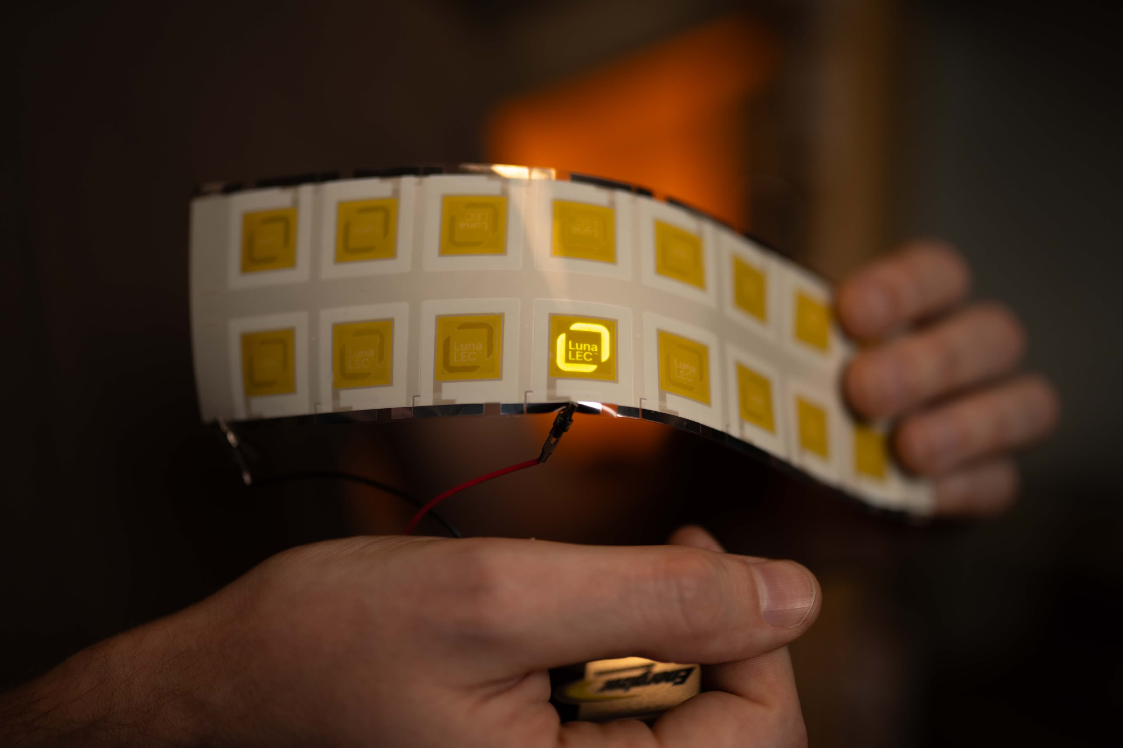
The LEC (or Light-emitting Electrochemical Cell as the full technical name) creates its light-emitting pn-junction structure in a different way. From a single layer consisting of a mix of carefully selected organic semiconductors and mobile ions, the LEC forms a pn-junction naturally through ion reorganization and electrochemical reactions while being powered. This means that a similarly intricate pn-junction structure as in LEDs and OLEDs can be achieved while only having to manufacture a single active layer. Sticking to solution processable organic materials, we can also formulate inks that can be deposited by standard printing techniques, increasing customizability, reducing cost and offering a more energy- and environmentally friendly manufacturing.
Our core knowledge and IP-portfolio of LEC operation, material selection, ink formulation and printing manufacturing allows us to develop this technology towards clear performance targets required by each product or application.
LED vs OLED vs LEC
Comparison
Property
LED
OLED
LEC
Manufacturing →
Semiconductor fab
Vacuum deposition
Printing in ambient air
Form Factor →
Rigid
Thin, Rigid / Flexible
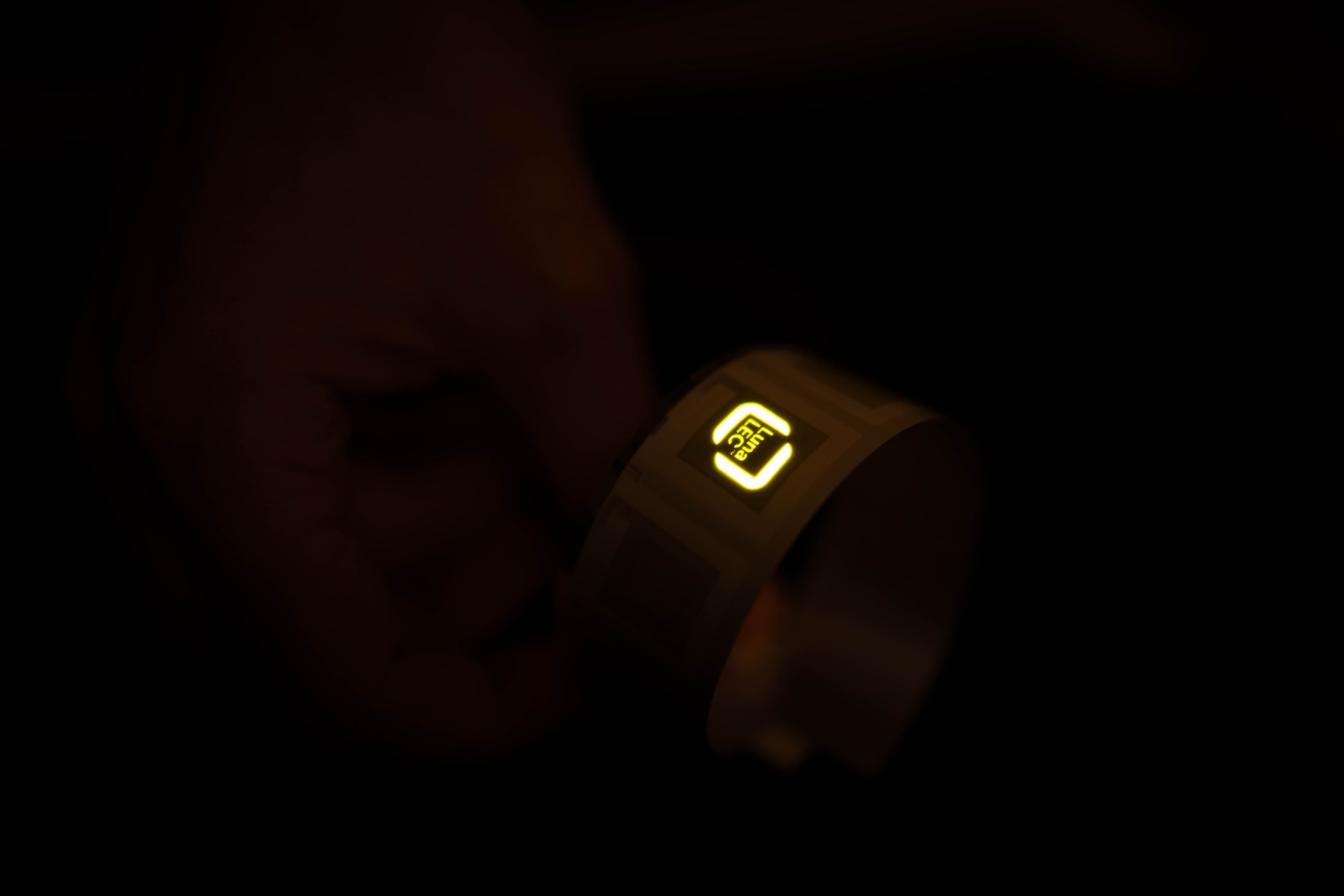
Ultra-thin, Flexible
Emission →
Point source
Area emission
Area emission
Emission pattern →
—
Expensive to customize
Easy to customize
Substrate →
Die, PCB
Glass, Plastic
Plastic, Foil, Glass
Material Cost →
Low
High
Very Low
Rare Earth →
Yes
Some
None
Manufacturing
LED
Semiconductor fab
OLED
Vacuum deposition
LEC
Printing in ambient air
Form Factor
LED
Rigid
OLED
Thin, Rigid / Flexible
LEC
Ultra-thin, Flexible
Emission
LED
Point source
OLED
Area emission
LEC
Area emission
Emission pattern
LED
—
OLED
Expensive to customize
LEC
Easy to customize
Substrate
LED
Die, PCB
OLED
Glass, Plastic
LEC
Plastic, Foil, Glass
Material Cost
LED
Low
OLED
High
LEC
Very Low
Rare Earth
LED
Yes
OLED
Some
LEC
None
Technical Data
Specifications
<250μm
Thickness
Total device stack
DC Voltage
Operation
Battery, NFC, RFID compatible
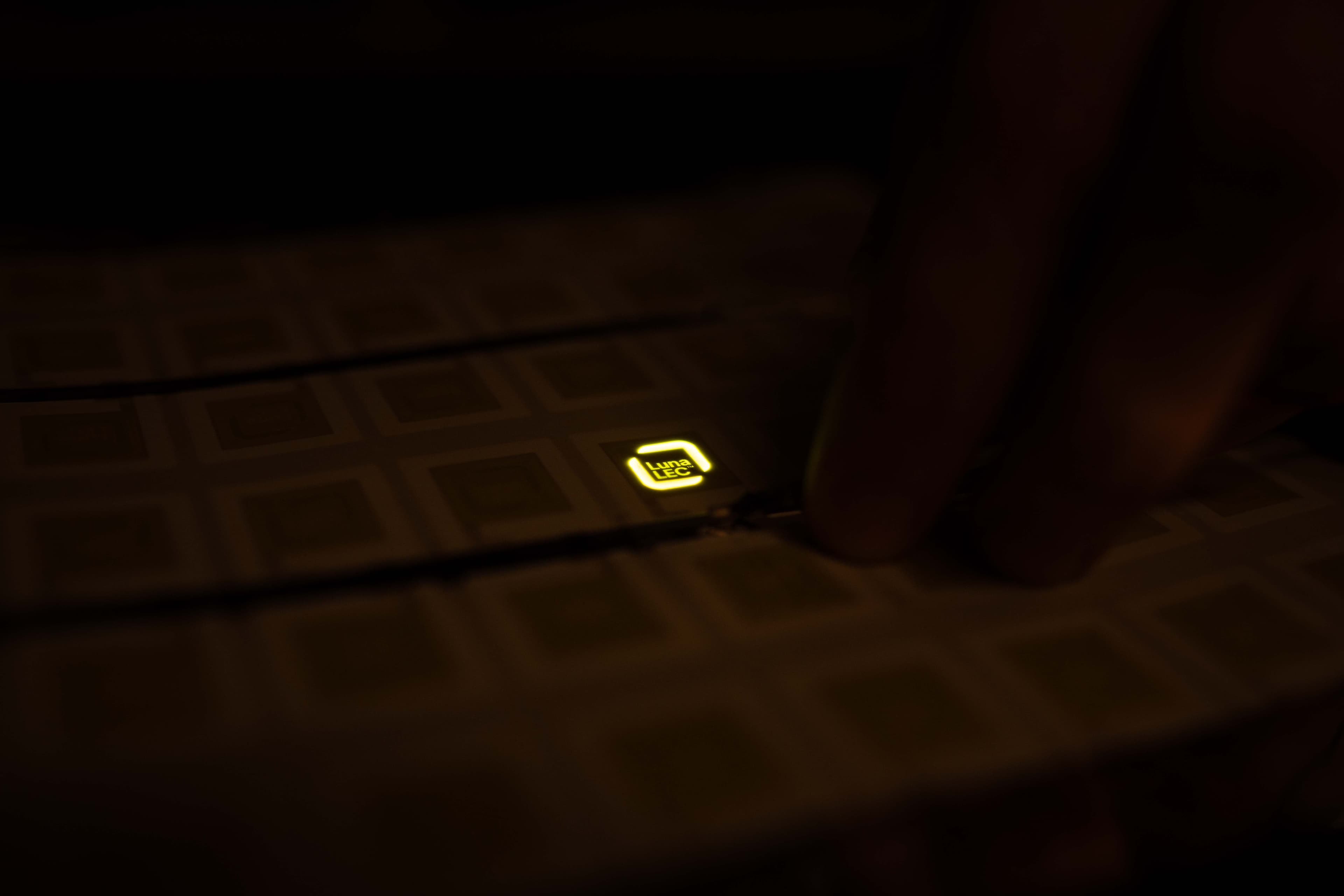
White
Emission
All colors available
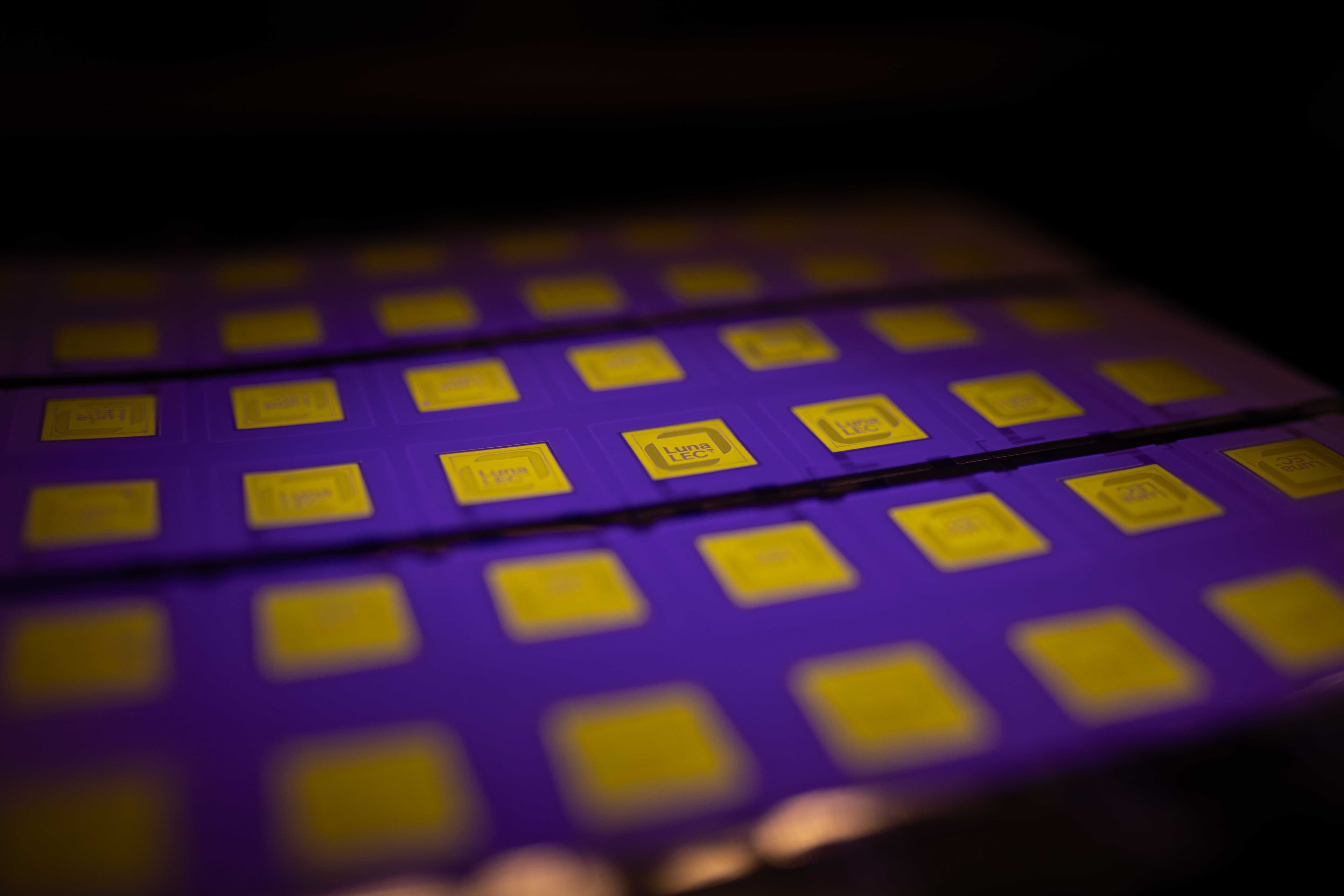
Manufacturing
Inkjet & screen printing

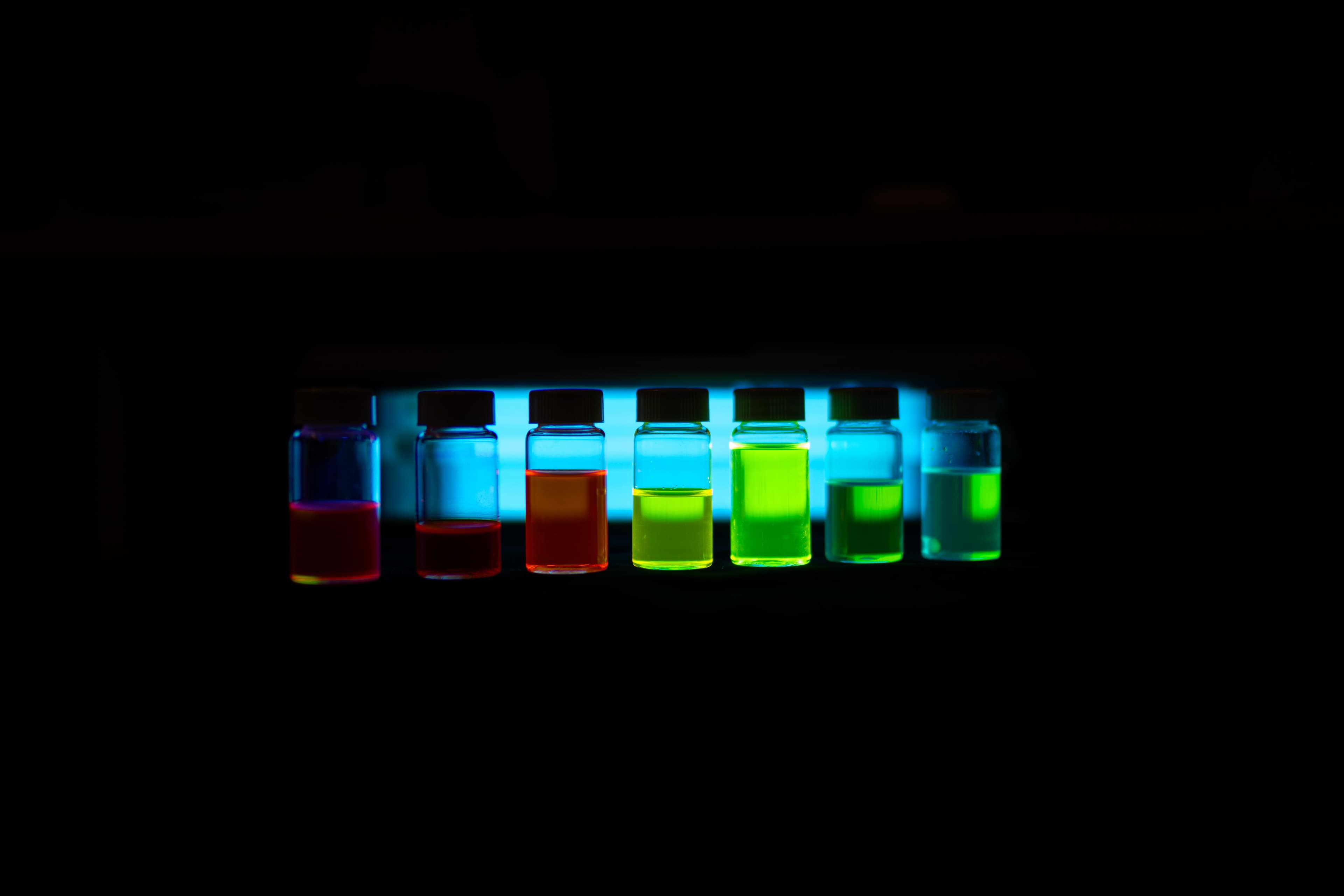
Across the Spectrum
Tunable color, formulated as ink.
Environmental Impact
Sustainability
Abundant Materials
Earth-abundant materials without rare earth elements or conflict minerals.
Low Energy
Solution-based printing requires less energy than traditional semiconductor manufacturing.
Material Efficient
Printing allows efficient material usage, greatly reducing material waste during manufacturing.
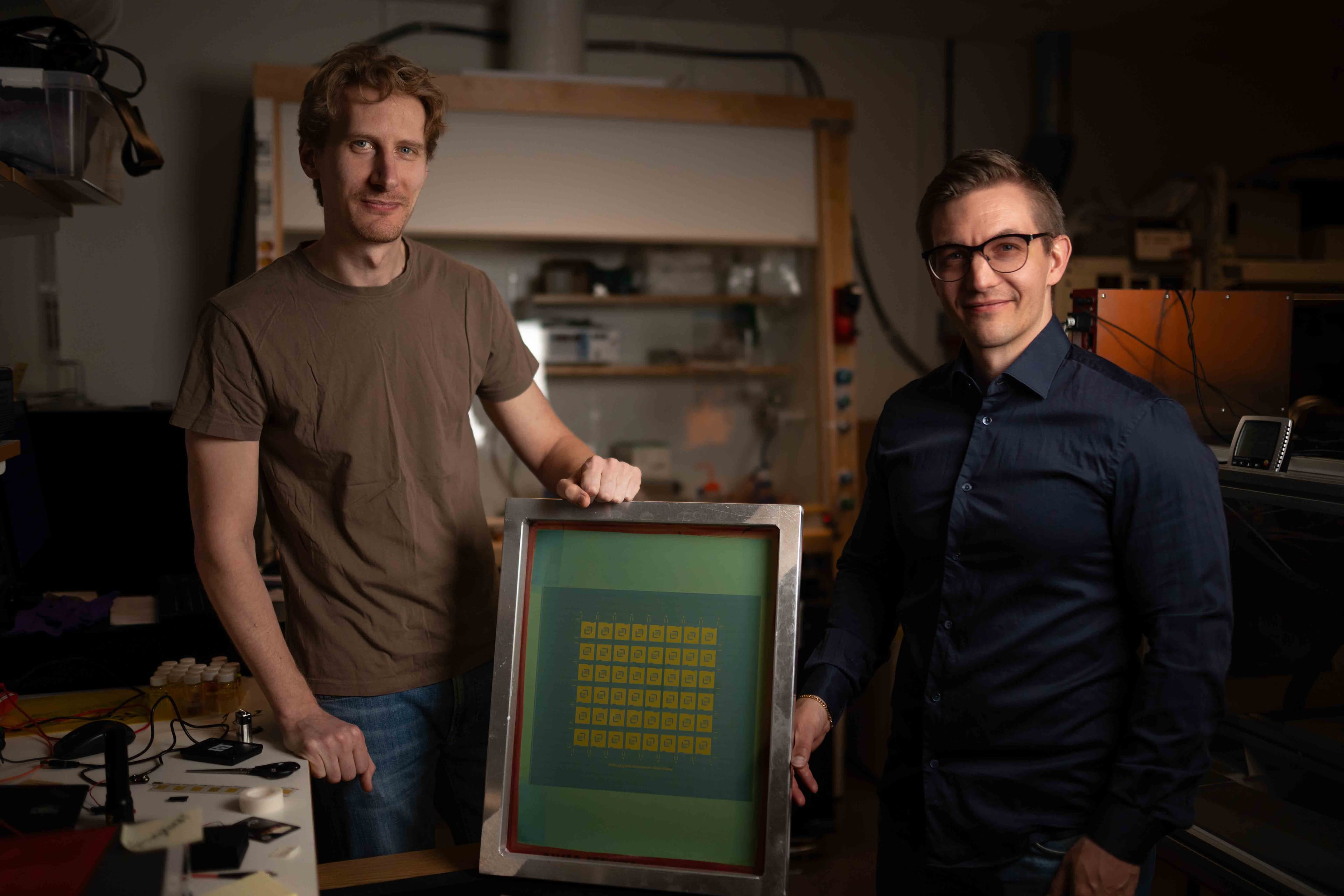
Behind the Scenes
From the Lab
A glimpse into our research and development process. From early prototypes to production-ready technology.
Get Started
Next Steps
Want to learn more about our technology?
Our team is ready to discuss how LEC technology can enable your next product innovation.